

Flip chip technology is an advanced semiconductor packaging and assembly method in which a semiconductor chip is mounted face-down onto a substrate, package carrier, or PCB. Unlike conventional wire bonding, where fine wires are used to connect the chip pads to the package, flip chip packaging uses solder bumps or other conductive bumps formed directly on the chip surface. These bumps create both electrical and mechanical connections between the chip and the substrate.
The term “flip chip” comes from the core process itself: after bumps are formed on the chip pads, the chip is flipped upside down so the bumped side faces the substrate. The chip is then aligned with the corresponding pads and bonded by solder reflow, eutectic bonding, or another controlled die attach process.
In modern IC packaging, flip chip technology is widely used where compact structure, shorter electrical paths, better thermal performance, and higher interconnection density are required. It is especially important for advanced packaging, AI computing chips, 5G communication devices, automotive electronics, memory chips, RF modules, optical modules, Mini/Micro LED, sensors, and high-end consumer electronics.
A Simple View of Flip Chip Technology
A simple way to understand flip chip technology is to divide it into four main steps: chip preparation, bumping, flipping, and packaging. Although actual production may involve more detailed operations such as wafer cleaning, inspection, flux dipping, underfill, and reliability testing, the basic principle remains the same.
1. Semiconductor Chip Preparation
The process begins with a semiconductor wafer after fabrication. Before individual chips are separated, the chip pads must be prepared for direct electrical connection. In traditional wire bonding, these pads are later connected by metal wires. In flip chip packaging, the pads need to receive bumps before the chip is mounted.
2. Bumping
Small solder bumps, copper pillars, gold bumps, or other conductive bumps are deposited onto the chip’s bonding pads. These bumps serve as connection points between the chip and the substrate or PCB. They provide the electrical path and also help form the mechanical joint during bonding.
Bumping is one of the key differences between flip chip and traditional wire bonding. In flip chip packaging, the wafer usually undergoes bumping before singulation. After that, the wafer is diced into individual dies for assembly.
3. Flip
After bumping and singulation, the die is picked and turned over so the bumped side faces downward. This is the step that gives flip chip technology its name. Because the connection points are now underneath the chip, the die bonder must align the chip very accurately with the substrate pads before bonding.
For fine-pitch packages, small alignment errors can lead to open circuits, solder bridging, weak joints, or yield loss. Therefore, high-precision vision alignment, stable motion control, and accurate bond force control are essential in flip chip assembly.
4. Packaging and Bonding
Once the flipped chip is aligned with the substrate or PCB, heat and controlled force are applied to form the connection. In many flip chip processes, solder reflow is used to melt the bumps and create a strong electrical and mechanical bond. Other processes may use eutectic bonding, flux dipping, pre-sintering, or thermal compression bonding depending on the package design and material system.
After bonding, underfill material is often introduced between the chip and substrate. Underfill helps reinforce the interconnects, reduce mechanical stress, and improve long-term package reliability, especially where thermal cycling or vibration may occur.
How Flip Chip Technology Differs from Wire Bonding
Flip chip technology is often understood by comparing it with conventional wire bonding. Both are IC packaging interconnection methods, but their structures and performance characteristics are different.
Wire Bonding Technology
In wire bonding, the semiconductor chip is first separated from the wafer through singulation. The chip is attached to a substrate, lead frame, or PCB using die attach adhesive. Then, thin metal wires are used to connect the chip pads to the package or board. After wire bonding, encapsulation or molding is usually applied to protect the chip and wires.
Wire bonding is mature, widely used, and relatively cost-effective. It is suitable for many standard semiconductor packages. However, the wire loops create longer electrical paths. As signal speed increases and package size becomes smaller, these longer paths may create limitations in high-frequency and high-density applications.
Flip Chip Technology
In flip chip packaging, the wafer is bumped before singulation. After the wafer is diced, each bumped die is flipped and directly mounted onto the substrate or PCB. The chip is connected through solder bumps or other bump structures instead of long wires.
This structure provides shorter electrical paths, lower parasitic effects, higher I/O density, and more efficient heat dissipation. Because the interconnects can be distributed across the chip surface rather than only around the chip edge, flip chip technology supports more compact and high-performance package designs.
| Comparison Item | Wire Bonding | Flip Chip Technology |
| Connection Method | Chip pads are connected by fine metal wires. | Chip pads are connected through solder bumps or conductive bumps. |
| Chip Orientation | Active side usually faces upward. | Active side faces downward toward the substrate. |
| Electrical Path | Longer due to wire loops. | Shorter and more direct. |
| Package Size | Requires space for wire loops and edge bonding. | More compact and suitable for high-density layouts. |
| Thermal Performance | Thermal path is more limited by package structure. | Heat can transfer more efficiently through direct chip-to-substrate contact. |
| Cost and Complexity | Lower cost and simpler process for many standard packages. | Higher process control requirements and higher equipment demands. |
| Typical Use | Standard ICs, mature packages, cost-sensitive devices. | Advanced ICs, AI chips, 5G, automotive electronics, memory, RF, optical modules, Mini/Micro LED. |
Flip Chip Configurations in IC Packaging
Flip chip technology can be used in different package structures. Two common configurations are chip-in-package and direct-chip-attach.
Chip-in-Package
In a chip-in-package structure, the flipped chip is mounted onto a package substrate first. The package is then assembled onto a PCB. This approach is widely used in advanced IC packaging because the intermediate substrate can provide routing, protection, and better package-level reliability.
Direct-Chip-Attach
In a direct-chip-attach structure, the flipped chip is directly attached to the PCB without an intermediate package substrate. This can reduce package size and shorten the interconnection path further, but it also requires careful control of board design, thermal expansion mismatch, underfill process, and assembly reliability.
Why Flip Chip Technology Is Used
Flip chip technology is not selected only because it is newer than wire bonding. It is used because it solves several packaging challenges that become more serious as chips become faster, smaller, and more complex.
· Shorter electrical paths: Direct bump connection reduces signal delay and parasitic effects.
· Higher I/O density: Interconnects can be distributed across the chip surface instead of only along the edge.
· Better high-frequency performance: Shorter paths are more suitable for RF, 5G, and high-speed devices.
· Improved thermal dissipation: The face-down structure can provide a more efficient heat transfer path.
· Smaller package size: Without wire loops, the package can be more compact.
· Better mechanical reliability: With proper underfill and bonding control, flip chip packages can withstand demanding operating conditions.
These advantages make flip chip packaging important for advanced semiconductor applications where wire bonding may no longer meet the performance, size, or reliability requirements.
Flip Chip Technology in 3D Integration
Flip chip technology also plays an important role in 3D integration. In a 3D integrated structure, different chips or functional layers can be separated and then connected in a vertical direction. This allows designers to use the third dimension for routing, interconnection, and functional separation.
For example, a sensitive device layer can be separated from control or readout circuits, while still maintaining short interconnect paths between different layers. This can reduce layout crowding and allow each chip or layer to be optimized independently. In advanced packaging, this idea is important for scaling beyond traditional planar architectures.
The same principle is valuable in semiconductor packaging applications such as stacked memory, multi-chip modules, SiP packaging, optical modules, and advanced heterogeneous integration. Instead of relying only on lateral routing, flip chip and stacked die processes make it possible to build more compact and functionally dense package structures.
Flip Chip LED Design as a Packaging Example
Flip chip technology is also used in LED packaging. In traditional LED packages, the chip may rely on wire bonding to connect the device to the package contacts. However, fine wires can become a reliability concern under mechanical stress, and the package structure can affect light output and thermal performance.
In a flip chip LED structure, the LED chip is inverted and connected directly through bottom-side contacts. This eliminates wire bonding, shortens the path from the junction to the package base, and can help improve thermal transfer. The result is a more compact LED package structure with fewer wire-related reliability risks.
For LED, optical module, Mini/Micro LED, and sensor-related packaging, the bonding process must maintain accurate placement while avoiding chip damage. This is where a high-precision die bonder becomes important. The equipment must support small chip handling, stable alignment, optional flux or dispensing processes, and repeatable bonding force.
Where Top-leading Die Bonders Fit Into Flip Chip Packaging
Flip chip technology depends heavily on die bonding equipment. A flip chip package may look simple in concept, but in production the process requires accurate chip picking, flipping, vision alignment, bonding force control, heating, flux management, and stable repeatability.
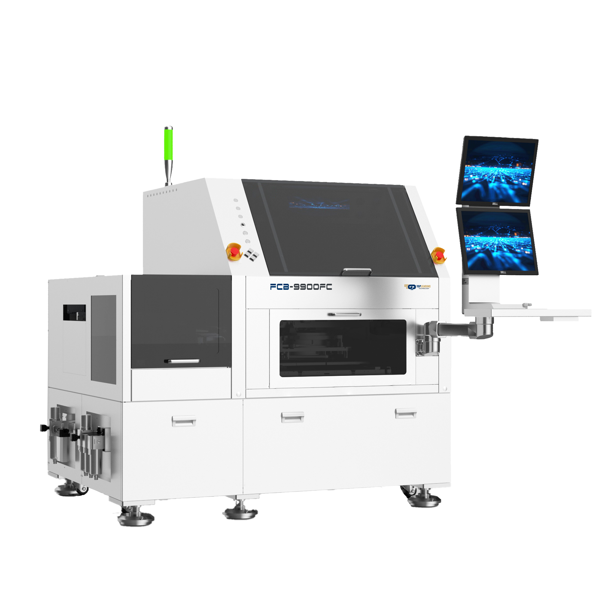
Top-leading provides automatic die bonding equipment for different flip chip and advanced packaging requirements. For high-volume flip chip production, the FCB9900FC Series High-Speed Flip-Chip Die Bonder is the main solution. It is designed for high-speed and high-precision flip chip processes, including flip chip reflow soldering, eutectic bonding, and pre-sintering.
The FCB9900FC Series uses a dual-gantry and dual-bond-head structure. It supports high-volume manufacturing for advanced packaging, AI computing chips, 5G communications, automotive electronics, high-end consumer electronics, and memory chip manufacturing. For production lines where throughput and alignment stability are both critical, this type of dedicated flip chip die bonder helps reduce manual intervention and improve process repeatability.
Key Capabilities Required for Flip Chip Die Bonding
Because flip chip assembly is more process-sensitive than conventional wire bonding, the die bonder must support more than basic pick-and-place. The following capabilities are especially important:
· High placement accuracy: Fine-pitch bumps must align with substrate pads precisely.
· Angular accuracy: Rotation error can affect bump-to-pad matching across the whole chip.
· Stable bond force: The equipment must prevent bump deformation and ultra-thin chip breakage.
· Flux dipping or flux spraying: Flux control affects solder wetting and joint quality.
· Heating and thermal compensation: Temperature changes can affect alignment and bonding consistency.
· Automatic calibration: Long-term production requires stable accuracy without drift.
· Carrier compatibility: Production may require 8-inch or 12-inch wafer rings, waffle packs, trays, strips, boats, or panels.
· High-speed material handling: Mass production needs automatic wafer loading, tray exchange, and reduced manual handling.
Top-leading FCB9900FC for High-Speed Flip Chip Assembly
The FCB9900FC Series High-Speed Flip-Chip Die Bonder is suitable when the flip chip process has moved from development into high-volume production. It supports chip sizes from very small dies to larger chips and is compatible with wafer rings, waffle packs, and trays.
Its key process features include:
· Dual gantry and dual bond head design for high-speed flip chip production
· High-precision XY placement and angular control
· Support for flip chip reflow soldering, eutectic bonding, pre-sintering, and flux dipping
· Automatic wafer loading and waffle pack tray exchange
· Thermal deformation compensation and automatic calibration
· One-key switching between face-up and flip chip bonding
· Flexible bond force control for ultra-thin and sensitive chips
For applications such as AI chips, 5G devices, automotive electronics, memory chips, and advanced IC packages, these functions help support stable output, yield control, and scalable production.
Other Top-leading Die Bonder Options for Related Applications
Not every customer needs a dedicated high-speed flip chip production line from the beginning. Some projects are still in process development, pilot production, micro-module assembly, optical module packaging, or stacked die packaging. In these cases, other Top-leading die bonder platforms may be more suitable.
PNP6600 Series Multi-Functional & High-Precision Die Bonder
The PNP6600 Series Multi-Functional & High-Precision Die Bonder is suitable for advanced semiconductor packaging, optical modules, power semiconductor modules, RF components, MEMS, sensor devices, and hybrid electro-optical packaging.
For projects that need high-precision die placement, epoxy or silver paste dispensing, glue dipping, spray dispensing, and optional flip chip capability, the PNP6600 Series provides a flexible platform for process development and high-reliability packaging.
PNP7000m/PNP7000mpro Series High-Speed Stacked Chip Die Bonder
The PNP7000m/PNP7000mpro Series High-Speed Stacked Chip Die Bonder is designed for memory chip manufacturing and stacked die production. It supports DAF multi-layer stacking, dispensing die attach, face-up bonding, and flip chip bonding options.
For Flash, LPDDR, DDR, controller chips, and multi-layer stacked packages, the bonding process must handle thin dies, high-speed motion, vibration control, and stable placement. This makes the PNP7000m Series suitable for stacked memory and advanced semiconductor packaging production.
PNP7000 LA Series High-Precision & Micro-Module Die Bonder
The PNP7000 LA Series High-Precision & Micro-Module Die Bonder is suitable for SiP, optical modules, RF/microwave components, Mini/Micro LED, sensors, automotive electronics, and compact micro-module packaging.
Its support for Uplook/Downlook vision, optional flux spraying, flip chip flux dipping, dispensing die bonding, and eutectic bonding makes it useful for high-density modules, small chips, ultra-thin substrates, and mixed packaging processes.
Common Applications of Flip Chip Technology
Flip chip technology is used across many semiconductor and electronics applications where performance, miniaturization, and reliability are important.
| Application | Why Flip Chip Is Used | Related Top-leading Equipment Focus |
| Advanced IC Packaging | Supports compact package structure, high I/O density, and short electrical paths. | FCB9900FC for high-speed flip chip bonding; PNP6600 for flexible process development. |
| AI Computing Chips | Requires high-density interconnection, efficient thermal path, and stable high-volume packaging. | FCB9900FC for high-speed and high-precision flip chip assembly. |
| 5G Communications | Needs high-frequency performance and compact RF package structure. | PNP7000 LA and PNP6600 for RF/microwave and micro-module bonding. |
| Memory Chips | Uses stacked die and high-throughput packaging structures. | PNP7000m/PNP7000mpro for stacked chip die bonding. |
| Optical Modules | Requires accurate placement of VCSEL, photodiodes, lenses, and submounts. | PNP6600 and PNP7000 LA for optical module die bonding. |
| Mini/Micro LED | Needs small chip handling, dense placement, and stable bonding force. | PNP7000 LA for micro-module and Mini/Micro LED bonding. |
| Automotive Electronics | Requires reliability under thermal and mechanical stress. | FCB9900FC, PNP6600, and PNP7000 LA depending on package type and production volume. |
What Buyers Should Consider When Selecting Flip Chip Die Bonding Equipment
When selecting equipment for flip chip packaging, it is not enough to compare only speed or accuracy. The right machine depends on the actual package structure, chip size, substrate type, bonding material, production stage, and yield requirement.
Key selection factors include:
· Chip size range: Confirm whether the machine supports micro-chips, standard dies, large dies, and ultra-thin chips.
· Substrate type: Check compatibility with strips, boats, panels, lead frames, carriers, ceramic substrates, PCBs, wafer rings, or trays.
· Bonding process: Determine whether the line needs flip chip reflow soldering, eutectic bonding, pre-sintering, dispensing, flux dipping, or flux spraying.
· Placement accuracy: Fine-pitch packages require stable micron-level alignment.
· Bond force range: Proper force control helps prevent chip cracking, bump damage, or poor contact.
· Thermal control: Heating capability and thermal compensation are important for reflow and eutectic processes.
· Automation level: R&D, pilot production, and mass production require different levels of automatic loading, tray exchange, and material handling.
· Process scalability: The equipment should support future product upgrades and capacity expansion.
Summary
Flip chip technology has become an important IC packaging method because it provides shorter electrical connections, better thermal performance, higher I/O density, and more compact package structures than traditional wire bonding. The process begins with chip preparation and bumping, followed by flipping, alignment, bonding, and often underfill reinforcement.
Compared with wire bonding, flip chip packaging is more suitable for high-speed, high-density, and advanced semiconductor applications. It also supports 3D integration, stacked die structures, direct-chip-attach designs, compact LED packages, optical modules, memory chips, RF devices, AI chips, 5G communication products, and automotive electronics.
However, flip chip technology also requires higher process control. Accurate alignment, stable bonding force, flux control, thermal compensation, and reliable underfill all affect final package performance. For this reason, choosing the right automatic die bonder is a key part of successful flip chip packaging.
Top-leading provides die bonding solutions for different flip chip and advanced packaging needs, including the FCB9900FC Series High-Speed Flip-Chip Die Bonder for high-volume flip chip production, the PNP6600 Series for high-precision multi-functional die bonding, the PNP7000m/PNP7000mpro Series for stacked memory chip bonding, and the PNP7000 LA Series for micro-module, optical module, RF, and Mini/Micro LED packaging.


